
Semiconductor
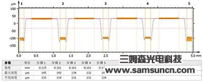
Wafer thickness and groove depth measurement
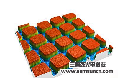
Silicon vias provide a primarily vertical metal connection to the silicon wafer. Using this technique it is possible to connect individual chips vertically through tiny copper wire structures. After the etching process is complete, these protrusions are called bumps. tsv structures are small holes with a high aspect ratio before they are filled, after which the bump grows on the surface of the silicon wafer. Both the depth of the tsv hole and the height of the bump can be measured by a spectral confocal sensor.
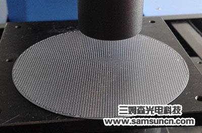
Wafer cutter thickness inspection, wafer cutter trench depth measurement
Surface profile scanning by 3D profilometer to analyse the surface height and microscopic profile of wafers
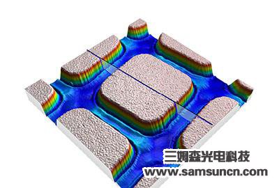
view of the surface topography
Trench depth and wafer surface height analysis diagram
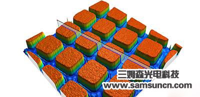
Wafer Surface Profile
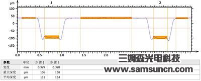
Wafer surface height analysis